Working principle of PN junction diode
Category: Electronics Articles
20 Mar 17
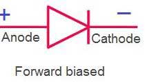
Forward bias of PN junction diode

- The diode is forward biased. The positive terminal of the battery is connected to the anode of a diode and negative terminal to the cathode.
- When battery is not connected, there is a barrier potential of 0.3 V for Silicon and 0.7 V for Germanium across the across the P-N junction of a diode.
- Due to majority charge carriers the external applied voltage of forward bias is opposed by the barrier voltage and the diode does not conduct the current.
- The applied voltage is increased above the barrier potential, it overcome the opposition of barrier potential and diode conducts the current due to majority carriers.
- This current is known as forward current and flows from anode to cathode through the diode.
- It is of the order of 20 to 50 mA at about 1V.
Reverse bias of PN junction diode

- The negative terminal of the battery is connected to the anode of a diode and positive terminal of battery is connected to cathode. Hence, the diode is reverse bias.
- When diode is reverse biased, majority carriers are blocked and only a small current flows through the diode due to the minority charge carriers.
- As the reverse voltage is increased from zero, the reverse current very quickly reaches its saturation value which is also called as leakage current or reverses saturation current.
- It is of the order of nanoamperes (nA) for Silicon and microamperes (µA) for Germanium.


