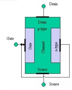
Construction of P-channel junction field effect transistor (JFET)
The construction diagram of P channel junction field effect transistor (JFET) is shown in above figure. Its construction is similar to the N channel JFET excepts that it consist of a P type silicon bar with two N type heavily doped regions diffused on opposites sides of its middle part. The JFET in which the current conduction takes place only due to holes as majority charge carriers is known as P channel JFET. The two PN junctions are form by the N region and the space between that is P region is called a channel. A single wire is taken in the form of the terminal when both the N type regions are connected internally known as the gate (G). The electrical connection which is also known as ohmic contact are made to both ends of the P type semiconductor and are taken out in the form of two terminals called drain (D) and source (S). The Drain (D) is a terminal through which electrons enter the semiconductor bar and from through which the electrons leave the semiconductor is source (S) terminal.


