Construction of photoconductive cells
It is based on the principle that the resistance of certain semiconductors materials decreases when they are exposed to radiations. In others words such material have high dark resistance and low irradiated resistance. The photoconductive cell is found that when radiations of sufficient energy fall on such photosensitive materials they cause the electrons to break away from their covalent bonds thereby generating electron hole pairs. These charge carriers are created within the material and reduce its resistance.The four materials normally used in photoconductive cells are cadmium sulphide (Cds), thalmium sulphide (TIS), cadmium salenide (CdSe) and lead sulphide (PbS).
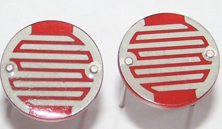
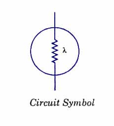
The simplified two dimensional model of cds cell is commonly used which is shown in figure 1 and the circuit the circuit symbol is shown in figure2.
The two electrodes are extended in an inter digital pattern in order to increase the contact area with the sensitive material. In this way it is possible to obtain a large ratio of dark to light resistance. An external power supply is necessary to generate a direction and provide a path for the current to flow. The value of applied voltage varies from a few volts to several hundred volts depending on photocell applications.


