What is solid state transformer
The conventional transformers had some disadvantages as well. The major among those disadvantages is power loss in the form of heat, especially during the summers. Also the cooper gets worn out with time and there are hysteresis losses as well. In order to overcome these problems and to achieve flawlessness, scientists devoted a lot of their time and energy to develop a new kind of transformers that are far better and effective than the primitive ones. They are known as Solid State Transformers.
“Several companies are working on technologies that could replace large traditional power transformers with power semiconductors and smaller transformers mounted on circuit boards. Although they are called solid-state transformers”, they are really power converters. A smart transformer is a solid-state device that serves as a power load with the ability to distribute and provide optimal power to loads.
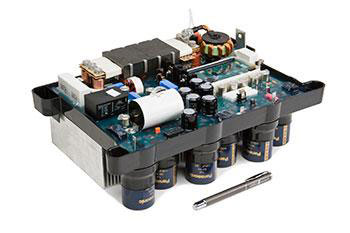
Solid-state transformer (SST) is a collection of high-powered semiconductor components, conventional high-frequency transformers and control circuitry which is used to provide a high level of flexible control to power distribution networks. By adding some communication capability, the entire package is often referred to as a smart transformer. SST technology can step up or step down AC voltage levels just like that of the traditional transformer but it also offers several significant advantages.
There’s been a lot of talk in the past few years about coming up with a solid-state version of the distribution transformer that now sits on utility poles in neighborhoods throughout the land. A solid-state transformer (SST) would be at least as efficient as a conventional version but would provide other benefits as well, particularly as renewable power sources become more widely used. Among its more notable strong points are on-demand reactive power support for the grid, better power quality, current limiting, management of distributed storage devices and a dc bus. It is starting to look more likely that we’ll see a practical SST design as GaN and SiC power
transistors with higher current and voltage ratings start coming to market and their prices drop.
A practical SST design could have an impact extending well beyond transformers for electrical utilities. SSTs could also find use is in variable-frequency drives for big induction motors. There have been several topologies suggested for SSTs but most being evaluated today are based around the idea of a dual active bridge (DAB) converter. A DAB uses a power bridge to modulate the incoming ac waveform into a high-frequency square wave. The square wave gets passed through a small high-frequency transformer to another power stage. This converter demodulates the square wave and sends it to another inverter which produces low-voltage ac. This scheme still uses a conventional transformer, but one optimized for higher frequencies (typically about 1 kHz).
This makes it much smaller and lighter than transformers optimized for ac line frequencies. The high-frequency transformer gives the SST galvanic isolation. It also has some leakage inductance in its primary and secondary windings, which also helps synthesize soft switching. During switching transients, transformer current resonates with the capacitors in parallel with switching devices, limiting the dv/dt and di/dt across the switches, thus reducing switching loss and boosting power efficiency. The fact that DAB converters have a symmetrical circuit configuration lets them handle bi-directional power flows, important when it comes to renewable sources sending power back up the grid. The power flow of a DAB converter can be controlled by varying the phase shift between those two bridges which changes the voltage across the transformer leakage inductance. Power transfers from the leading bridge to the lagging bridge.
One of the difficulties in fabricating a SST is that the 7.2-kV line voltages that characterize distribution power lines exceed the operating voltage of today’s 6.5 kV. So multiple devices must be used in series to keep below the operating maximum. A prototype uses a topology that includes a seven-level cascaded H-bridge for the high voltage rectifier stage. There are other difficulties as well. One is that the minimum current rating for the 6.5-kV insulated gate bipolar transistors (IGBTs) is 200 A. This is too large for the 20 kVA transformer with an input current of only about 3 Arms. Thermal issues also affect the SST’s operation, which has forced researchers to come up with special packaging for their 25-A IGBTs. Additionally, the team had to come up with a way to isolate IGBT drivers for both power supply and gating signals. To sense the 7.2 kVac voltage, the researchers devised a sensor that was compact and which incorporated high-voltage isolation because existing models were too large and not isolated from the high input voltage.
Finally, they had to get around the fact that the insulation capability for 6.5-kV IGBT is 10.2 kV, but the high-voltage-side dc bus voltage is 11.4 kV. They ended up floating the heatsink for each 6.5-kV IGBT while maintaining ample clearance and creepage distance between the heatsinks. To keep the voltage across input inductor down to manageable levels, the team built eight identical inductors and put them in series so the maximum voltage stress for each of them is just 0.9 kV. Researchers have also developed a prototype using 15 kV SiC MOSFET/JBS diodes. They are not trying to identify other major issues related to implementing a high-voltage system using SiC power devices, including the challenges in designing a system to support high dV/dt and dI/dt, and to design an efficient and compact high-frequency transformer.


