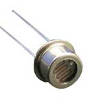
- The PIN diode is a diode with a wide, it lightly doped intrinsic semiconductor region between a p- type semiconductor and an n-type semiconductor region.
- This region normally heavily doped as they are used for ohmic contacts.
- The wide intrinsic region is in difference to an ordinary PN diode.
- The intrinsic region makes the diode an inferior rectifier, but it makes the diode suitable for fast switches, photo detector, attenuators, and high voltage power electronics application.

Construction of PIN diode:

A PIN diode is made up of three semiconductor materials. The intrinsic semiconductor separated by two heavily doped p and n type semiconductor material. The intrinsic layer of the diode is the one that provides the change in properties which compared to normal PN junction diode. The intrinsic region offers high resistance to the current flowing through it.
Operation of PIN diode:
The PIN diode exactly same as a normal diode It operates in under what is called as high level injection. Its function can be likened to filling up a water bucker with a hole on the side. It will begin to pour out when the water reaches the hole’s level. Once the flooded electrons and holes reach an equilibrium point the diode will conduct current. The number of elections is equal to the number of holes in the intrinsic region. When the PIN diode is connected in forward biased, the charge carries are very much higher than level of intrinsic carriers attention. Due to this reason the electric field the high level injection level extends deeply into the region, this electric field assists in speeding up the moving of charge carries from P and n region, which consequences in quicker operation of the PIN diode, making it an appropriate device for high frequency operation.