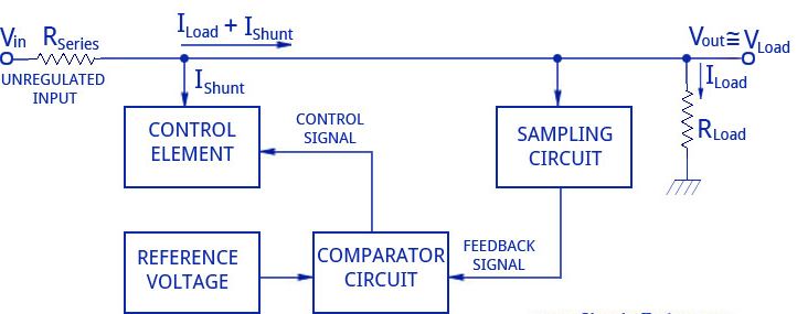
Block diagram of transistor shunt voltage regulator
The block diagram of transistor shunt voltage regulatoris shown in above figure. The transistor shunt voltage regulator is a control element connected in parallel with the load due to this circuit is called a shunt voltage regulator. The unregulated DC voltage is obtained from a rectifier and filter combination. The total current supplied by the unregulated input Vin is shared by the load RL and the control element. The control flowing through the control element is IShunt. The sampling network samples the output voltage VOut and provides a feedback signal proportional to the output voltage VOut to the comparator circuit. The comparator circuit compares the feedback signal with a constant reference voltage to produce a control signal which is applied to the control circuit. Depending upon this control signal, the control element will change its current IShunt in such a way that any changes in the output voltage are multiplied to maintain the output voltage control. If the output voltage increases above the regulated value VOut then the sampling networks provides the increase feedback voltage. This will force the comparator circuit to increase the control signal amplitude. This will, in turn, force the control current to draw more current IShunt. Therefore the load current ILoad will decrease and the output voltage will be brought back to the regulated value VOut. If the load voltages decrease then exactly opposite action will take place to regulate the output voltage. This voltage regulator is preferred for the fixed voltages application only.


